

It is always important to choose the correct tool for the job, and choosing the correct interface for high-frequency electromagnetic simulations is no different. In this blog post, we take a simple example of a plane wave incident upon a dielectric slab in air and solve it in two different ways to highlight the practical differences and relative advantages of the Electromagnetic Waves, Frequency Domain interface and the Electromagnetic Waves, Beam Envelopes interface.
Meshing Free Space in Two Electromagnetic Interfaces
Both of these interfaces solve the frequency-domain form of Maxwell’s equations, but they do it in slightly different ways. The Electromagnetic Waves, Frequency Domain interface, which is available in both the RF and Wave Optics modules, solves directly for the complex electric field everywhere in the simulation. The Electromagnetic Waves, Beam Envelopes interface, which is available solely in the Wave Optics Module, will solve for the complex envelope of the electric field for a given wave vector. For the remainder of this post, we will refer to the Electromagnetic Waves, Frequency Domain interface as a Full-Wave simulation and the Electromagnetic Waves, Beam Envelopes interface as a Beam-Envelope simulation.
To see why the distinction between Full-Wave and Beam-Envelope is important, we will begin by discussing the trivial example of a plane wave propagating in free space, as shown in the image below. We will then apply the lessons learned to the dielectric slab.
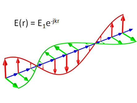
A graphical representation of a plane wave propagating in free space, where the red, green, and blue lines represent the electric field, magnetic field, and Poynting vector, respectively.
To properly resolve the harmonic nature of the solution in a Full-Wave simulation, we need to mesh finer than the oscillations in the field. This is discussed further in these previous blog posts on tools for solving wave electromagnetics problems and modeling their materials. To simulate a plane wave propagating in free space, the number of mesh elements will then scale with the size of the free space domain in which we are interested. But what about the Beam-Envelopes simulation?
The Beam-Envelopes method is particularly well-suited for models where we have good prior knowledge of the wave vector, \mathbf{k}. Practically speaking, this means that we are solving for the fields using the ansatz \mathbf{E}\left(\mathbf{r}\right) = \mathbf{E_1}\left(\mathbf{r}\right)e^{-j\mathbf{k_1}\cdot\mathbf{r}}. Notice that the only unknown in the ansatz is the envelope function \mathbf{E_1}\left(\mathbf{r}\right). This is the quantity that needs to be meshed to obtain a full solution, hence the mention of beam envelopes in the name of the interface. In the case of a plane wave in free space, the form of the ansatz matches exactly with the analytical solution. We know that the envelope function will be a constant, as shown by the green line in the figure below, so how many mesh elements do we need to resolve the solution? Just one.
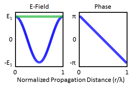
The electric field and phase of a plane wave propagating in free space. In the field plot (left), the blue and green lines show the real part and absolute value of E(r), which are abs(\mathbf{E_1}\left(\mathbf{r}\right)e^{-j\mathbf{k_1}\cdot\mathbf{r}}) = E_1 and real(\mathbf{E_1}\left(\mathbf{r}\right)e^{-j\mathbf{k_1}\cdot\mathbf{r}}) = E_1\cos(kr), respectively. The phase plot (right) shows the argument of E(r). In both plots, the x-axis is normalized to a wavelength, so this represents one full oscillation of the wave.
In practice, Beam-Envelopes simulations are more flexible than the \mathbf{E}\left(\mathbf{r}\right) = \mathbf{E_1}\left(\mathbf{r}\right)e^{-j\mathbf{k_1}\cdot\mathbf{r}} ansatz we just used. This is for two reasons. First, instead of specifying a wave vector, we can specify a user-defined phase function, \phi\left(\mathbf{r}\right) = \mathbf{k}\cdot\mathbf{r}. Second, there is also a bidirectional option that allows for a second propagating wave and a full ansatz of \mathbf{E}\left(\mathbf{r}\right) = \mathbf{E_1}\left(\mathbf{r}\right)e^{-j\phi_1\left(\mathbf{r}\right)} + \mathbf{E_2}\left(\mathbf{r}\right)e^{-j\phi_2\left(\mathbf{r}\right)}. This is the functionality that we will take advantage of in modeling the dielectric slab (also called a Fabry-Pérot etalon).
The points discussed here will come up again in the dielectric slab example, and so we highlight them again for clarity. The size of mesh elements in a Full-Wave simulation is proportional to the wavelength because we are solving directly for the full field, while the mesh element size in a Beam-Envelopes simulation can be independent of the wavelength because we are solving for the envelope function of a given phase/wave vector. You can greatly reduce the number of mesh elements for large structures if a Beam-Envelopes simulation can be performed instead of a Full-Wave simulation, but this is only possible if you have prior knowledge of the wave vector (or phase function) everywhere in the simulation. Since the degrees of freedom, memory used, and simulation time all depend on the number of mesh elements, this can have a large influence on the computational requirements of your simulation.
Meshing a Dielectric Slab in COMSOL Multiphysics
Using the 2D geometry shown below, we can clearly see the different waves that need to be accounted for in a simulation of a dielectric slab illuminated by a plane wave. On the left of the slab, we have to account for the incoming wave traveling to the right, as well as the reflected wave traveling to the left. Because of internal reflections inside the slab itself, we have to account for both left- and right-traveling waves in the slab, and finally, the transmitted waves on the right. We also choose a specific example so that we can use concrete numbers.
Let’s make the dielectric slab an undoped silicon (Si) wafer that is 525 µm thick. We will simulate the response to terahertz (THz) radiation (i.e., submillimeter waves), which encompasses wavelengths of approximately 1 mm to 100 µm and is increasingly used for classifying semiconductor properties. The refractive index of undoped Si in this range is a constant n = 3.42. We choose the domain length to be 15 mm in the direction of propagation.
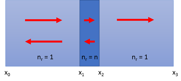
The simulation geometry. Red arrows indicate incident and reflected waves. The left and right regions are air with n = 1 and the Si slab in the center has a refractive index n = 3.42. The xis on the bottom denote the spatial location of the planes. The slab is centered in the simulation domain, such that x1 = (15 mm – 525 µm)/2. Note that this image is not to scale.
For a 2D Full-Wave simulation, we set a maximum element size of \lambda/8n to ensure the solution is well resolved. The simulation is invariant in the y direction and so we choose our simulation height to be \lambda/(8\times3.42). Because we have constrained the wave to travel along the x-axis, we choose a mapped mesh to generate rectangular elements. The mesh will then be one mesh element thick in the y direction, with a mesh element size in the x direction of \lambda/8n, where n depends on whether it is air or Si. Again, note that this is a wavelength-dependent mesh.
Before setting up the mesh for a Beam-Envelopes simulation, we first need to specify our user-defined phase function. The Gaussian Beam Incident at the Brewster Angle example in the Application Gallery demonstrates how to define a user-defined phase function for each domain through the use of variables, and we will use the same technique here. Referring to x0, x1, and x2 in the geometry figure above, we define the phase function for a plane wave traveling left to right in the three domains as
where n = 3.42 and the first line corresponds to \phi in the leftmost domain, the second line is \phi in the Si slab, and the bottom line is \phi in the rightmost domain. We then use this variable for the phase of the first wave, and its negative for the phase of the second wave. Because we have completely captured the full phase variation of the solution in the ansatz, this allows a mapped mesh of only three elements for the entire model — one for each domain. Let’s examine what the mesh looks like in the Si slab for these two interfaces at two different wavelengths, corresponding to 1 mm and 250 µm.
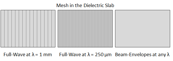
The mesh in the Si (dielectric) slab. From left to right, we have the Full-Wave mesh at 1 mm, the Full-Wave mesh at 250 µm, and the Beam-Envelopes mesh at any wavelength. Note that the Full-Wave mesh density clearly increases with decreasing wavelength, while the Beam-Envelopes mesh is a single rectangular element at any wavelength.
Yes, that is the correct mesh for the Si slab in the Beam-Envelopes simulation. Because the ansatz matches the solution exactly, we only need three total elements for the entire simulation: one for the Si slab and one each for the two air domains on either side of it. This is independent of wavelength. On the other hand, the mesh for the Full-Wave simulation is approximately four times more dense at \lambda = 250 µm than at \lambda = 1 mm. Let’s look at this in concrete numbers for the degrees of freedom (DOF) solved for in these simulations.
|
Wavelength Simulated |
Full-Wave Simulation DOF Used |
Beam-Envelopes Simulation DOF Used |
|---|---|---|
| 1 mm | 4,134 | 74 |
| 250 µm | 16,444 | 74 |
The number of degrees of freedom (DOF) used at two different wavelengths for the Full-Wave and Beam-Envelopes simulations.
Again, it is important to point out that this does not mean that one interface is better or worse than another. They are different techniques and choosing the appropriate option is an important simulation decision. However, it is fair to say that a Full-Wave simulation is more general, since we did not need to supply it with a wave vector or phase function. It can solve a wider class of problems than Beam-Envelopes simulations, but Beam-Envelopes simulations can greatly reduce the DOF when the wave vector is known. As we have seen in a previous blog post, memory usage in a simulation strongly depends on the number of DOF. Do not blindly use a Beam-Envelopes simulation everywhere though! Let’s take a look at another example where we intentionally make a bad choice for the wave vector and see what happens.
Making Smart Choices for the Wave Vector
In the hypothetical free space example above, we chose a unidirectional wave vector. Here, we will do the same for the Si slab. It is important to emphasize that choosing a single wave vector where we know that the solution will be a superposition of left- and right-traveling waves is an exceptionally bad choice, and we do this here solely for demonstration purposes. Instead of using the bidirectional formulation with a user-defined phase function, let’s naively choose a single “guess” wave vector of \mathbf{k_G} = n\mathbf{k_0} = \mathbf{k} and see what the damage is. Using our ansatz, inside of the dielectric slab we have
where the left-hand side is the solution we are computing and the right-hand side is exact. Now, we manipulate the equation slightly to examine the spatial variation in the solution.
We intentionally chose the case where \mathbf{k_G} = \mathbf{k}, which means we can simplify to
Since \mathbf{E_1} and \mathbf{E_2} are constants determined by the Fresnel relations at the boundaries of the dielectric slab, this means that the only spatial variation in the computed solution will come from exp\left(-j\left(\mathbf{k+k_G}\right)\cdot\mathbf{r}\right). The minimum mesh requirement in the slab is then determined by the “effective” wavelength of this oscillating term
which is half of the original wavelength. Not only have we made the Beam-Envelopes mesh wavelength dependent, but the required mesh in the dielectric slab for this choice of wave vector needs to be twice as dense as the mesh for a Full-Wave simulation. We have actually made the situation worse with the poor choice of a single wave vector for a simulation with multiple reflections. We could, of course, simply double the mesh density and obtain the correct solution, but that would defeat the purpose of choosing the Beam-Envelopes simulation in the first place. Make smart choices!
Simulation Results
Another practical question is how do the results of a Full-Wave and Beam-Envelopes simulation compare? They are both solving Maxwell’s equations on the same geometry with the same material properties, and so the various results (transmission, reflection, field values) agree as you would expect. There are slight differences though.
If you want to evaluate the electric field of the right-propagating wave in the dielectric slab, you can do that in the Beam-Envelopes simulation. This is, of course, because we solved for both right- and left-propagating waves and obtained the total field by summing these two contributions. This could be extracted from the Full-Wave simulation in this case as well, but it would require additional user-defined postprocessing and may not be possible in all cases. It may seem counterintuitive in that we actually have more information readily available from a Beam-Envelopes simulation, even though it is computationally less expensive. We must remember, however, that this is simply the result of solving the model using the ansatz we specified initially.
Concluding Thoughts on Interfaces for High-Frequency Modeling
We have examined the simple case of a dielectric slab in free space using both the Electromagnetic Waves, Frequency Domain and Electromagnetic Waves, Beam Envelopes interfaces. In comparing Full-Wave and Beam-Envelopes simulations, we showed that a Beam-Envelopes simulation can handle much larger simulations, but only in cases where we have good knowledge of the wave vector (or phase function) everywhere in the simulation. This knowledge is not required for a Full-Wave simulation, but the simulation must then be meshed on the order of a wavelength, as opposed to meshing the change in the envelope function in a Beam-Envelopes simulation. It is also worth mentioning that most Beam-Envelopes meshes will need more than the three elements shown here. This was only possible here because we chose a textbook example with an analytical solution to use as a teaching model. For more realistic simulations, you can refer to the Mach-Zehnder Modulator or Self-Focusing Gaussian Beam examples in the Application Gallery.
Note that the Electromagnetic Waves, Frequency Domain interface is available in both the RF and Wave Optics modules, although with slightly different features. The Full-Wave simulation discussed in this post could be performed in either module, although the Beam-Envelopes simulation requires the Wave Optics Module. For a full list of differences between the RF and Wave Optics modules, you can refer to this specification chart for COMSOL Multiphysics products.
Further Resources
- Check out these related blog posts:
- Watch these videos:
- Take your electromagnetics modeling to the next level at a local training event
- Contact us with questions about your own model

Comments (0)